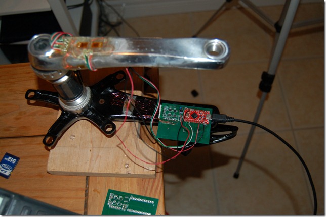
Why is the Left crank arm of V2 connected to V3 via frankenwiring? I was experiencing some very peculiar ADC behaviour. It’s hard to see, but next to the LM-4140 reference is now a blue capacitor. Turns out it was drifting very very high and erratically so that as the load changed so did the output. I missed the 0.1uF capacitor that was supposed have been after the regulator. I’ll need to recalibrate it but things are now a bit more stable. I’ve been asked about releasing PCB schematics. I’m not decided on this but this is a good reason not, to at least not yet. I also hold that without training installing strain gauges is a recipe for disaster and wasted money.
Power consumption is still an issue and with the drifting reference voltage solved, I was able to rewrite my “readadcR” routine to the “wiggle” version. My naming conventions aren’t all that sane when testing (I’m “wiggling” on and off a random pin). However interrupting the transfer to switch a pin didn’t impact the overall readout. According to the datasheet it shouldn’t but until it’s tested I believe nothing.
short readadcR() {
  digitalWrite(slaveSelectPinR,LOW);   // take the SS pin low to select the chip:
  byte one = SPI.transfer(0xFF);  //  send in the address and value via SPI:
  byte two = SPI.transfer(0xFF);
  byte three = SPI.transfer(0xFF);
  digitalWrite(slaveSelectPinR,HIGH);   // take the SS pin high to de-select the chip:
  return (one << 14 | two << 6 | three >> 2); //output the value from the three bytes as one short
}

short readadcRwiggle() {
  digitalWrite(slaveSelectPinR,LOW);   // take the SS pin low to select the chip:
  digitalWrite(wiggle,HIGH);
  byte one = SPI.transfer(0xFF);  //  send in the address and value via SPI:
  digitalWrite(wiggle,LOW);
  byte two = SPI.transfer(0xFF);
  byte three = SPI.transfer(0xFF);
  digitalWrite(slaveSelectPinR,HIGH);   // take the SS pin high to de-select the chip:
  return (one << 14 | two << 6 | three >> 2); //output the value from the three bytes as one short
}
Running the two routines (one reads and averages 10 values then the next routine does the same)yielded the above graph. Very little difference. The difference between the two techniques is highlighted below.
It’s obvious that at times the readings are slightly different, but this is on a 65000 value scale and averaged out the difference was 0.38 bits. Pretty insignificant as this should just be the last few bits plus a little offset for reading 10 values then reading 10 other values causing some error as I dynamically load the device.
What does this mean. Earlier here, I showed that currently I’m at 34ma, 17 - 19ma is the bridge itself! That is much too high! I’m targeting a lower value and V4 might not be perfect but it needs to be in the single digits at least. So assuming that reading the ADC takes 3/4 of the time and calculations take 1/4, and there are 3 read periods and only 1 bridge needs to be active for 1/3 of the reading that means that 19ma *1 bridge/2bridges * 1/4 duty cycle = 2.37ma.
Okay, so we dropped 19 to 2.37ma but we can still do better. If I added a minor delay to reduce read cycles in half (8000/s per side totalling 16000 samples/s) we drop both the bridge and the ADC’s to 1.185 and the adc to 0.4ma. This should in turn put the microcontroller to sleep for effectively half the time, dropping it from 17 to 8. I suspect this is wrong due to the regulator drawing more power.
So current consumption would be at about 10.5ma so far for V4. that should give about 20 – 22 hours of operation. A far cry from Quarq’s 300 hours. I suspect that they must reduce read rates even further leading me to question how much more accurate these devices could be if they scarified operating time. Original Quarq Saturn is listed at 400 hours on a 600mah battery. Total consumption when in operation is just over 1 ma. This is brutally low as I’m still not dealing with the ANT+ current consumption, however that is very very low.


No comments:
Post a Comment