“We have to continually be jumping off cliffs and developing our wings on the way down.” - Kurt Vonnegut
Since Friday (July 5th) I’ve jumped off of a lot of cliffs. About 9/10 times my “wings” didn’t work, leaving me to ask why. Okay, enough with the metaphors. On to ramblings about solder reflow and where my prototype boards are.
Stencil
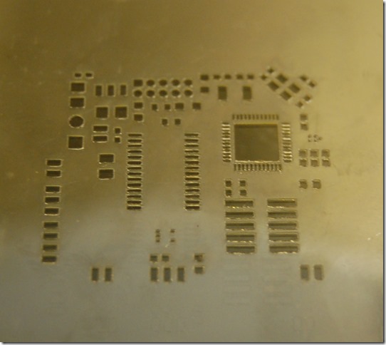
The first package I received was the stencil for the solder paste.

I thought, “looks good” but I wasn’t sold on the Balun BGA holes nor was I keen on the QFN. Pololu did a good job sorting out that I sent the wrong file, but here’s the problem (beside 25 dollars being a bit high for a laser cut mylar stencil).
- Stencil = $24 dollars USD
- Shipping = $29.95 dollars USD
- Fedex processing 13% tax = 14.97
Reflow Toaster Oven


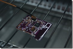
Above, the reflow oven hacked together. The side panel is still off but it seems to work well. I tested with some old boards as seen below:


Accuity V4 Boards
Everything having gone very well, including reflowing a AP2 module that had ruin solder pads which acctually connected up perfectly, I moved on to the Accuity boards. Using the stencil, and making many attempts to get all the pads filled and separated, I populated the board with tweezers.
I avoided placing a few parts, mainly the ADS1248 due to their 13 – 14 dollar price assuming I’ll mess this up several times. Mess it up I did.


After 2 attempts I think I realized that something was inherently wrong when the debugger couldn’t talk to these. I doubted myself and and thought the circuit was wrong or broken. Dreading a 30 day lead time I kept forging ahead speculating that the thermal relief pad had too much solder. As a result I pre-soldered the board and the package rather than using solder paste. I had seen this technique in a hot air reflow video. Failure, but it was obvious that there was too much solder on the thermal relief pad.
In test 4 I used the reflow method but only installed a few chips with barely any solder paste on the centre thermal pad. I ended up with bridged connections on my pins though. I cleaned it up with solder wick, flux, and solder, reflowed it again and it finally connected to the debugger!

One of the things that aided me was increasing the maximum temperature dwell time (I think?). However, it will not transmit wirelessly. There is a simple reason. The Balun will not reflow!
It’s small, 1mm x 1.5mm with 5 ball BGA array. The stencil can’t be used in the area of the QFN and the solder past is stuck in the BGA holes. You really need a stainless steel or aluminium stencil for these.
I’ve made about 6 attempts with this board and the board still works but the Balun will not solder. I have a single $1.50 Balun left to attempt with tonight and suspect I’ll just have to order more.
To sort the QFN issue I have a professional QFN kit on order from Protoadvantage, but I have only one solution for the Balun. DELETE the Balun. I’m sorry ST Micro. I might contact them for advice, but at this point I’m too frustrated.
It’s not worth it. The space savings is too ambitious and it’ll have a high wastage at the hobbist scale! The balls pop off when I attempt to reflow it, or they bridge, or it’s not enough paste and falls off never to be seen again. It’s too small to use at this level. A professional could easily do it, but a reflow oven in a home without a pick and place machine or a stainless stencil held in place by a computer controlled robot -- Without ALL of that it is as close to impossible as you can get without declaring it.
Also, 0402 is a small size. I’ve gotten used to it but you’ll want to make sure you space your pads a bit better than I did in some places if you want to use a mylar stencil. Mylar stencils budge up on the sides making it very hard for the paste to not bridge. Lifting “vertical” is impossible as you normally tape down an edge. This makes it more difficult as well.
One attempt tonight, and honestly I’m glad I’m down to one Balun, but I do not want to waste another month waiting on circuit boards. A 6:1 ratio is proving to not give me enough margin to build one board. I’ve been told I have patience, I think it’s closer to OCD.
At a hobby level, it's easier not to use solder paste with small-pitch BGA devices like that balun but just use flux. The balls provide sufficient solder to attach the part. Use a "tacky flux" to get the part to stick before you reflow.
ReplyDeleteHi Janek,
ReplyDeleteI learned that first hand. I redesigned the board copying nordic's antenna and balun used on their DK and EK. This is working pretty well. I think I'm going to stick to this instead of pursuing the ST Balun further. I had the space to spare on the board so it wasn't a major loss.
A couple things from my experience with the nRF chip:
ReplyDelete* There's a Johanson balun specifically for the Nordic chips that's not a BGA part. I've had good luck reflowing this by hand. http://www.johansontechnology.com/rfbaluns and search for Nordic.
* Have you tried oshstencils.com? Not sure what shipping would be like to Canada, but the quality is good.